Similarly, photoresist can be functionally divided into positive and negative photoresist: the exposed part of the positive photoresist will dissolve in the developer after photochemical reaction, while the unexposed part will not dissolve in the developer, and will remain on the substrate to copy the same figure on the mask onto the substrate; The exposed part of the negative photoresist is insoluble in the developer due to cross-linking and curing, while the unexposed part dissolves in the developer, and copies the pattern opposite to the mask onto the substrate.
(1) Photoresist composition

(2) reactive principles of positive and negative photoresist
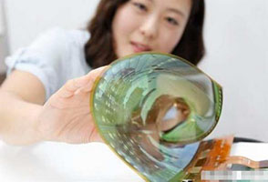
Photoresist can be divided into printed circuit board (PCB) photoresist, liquid crystal display (LCD) photoresist, semiconductor photoresist, and other photoresist according to the field of application. PCB photoresist has a lower technical barrier than the other two types, while semiconductor photoresist represents the most advanced level of photoresist technology.
3) Photoresist classification under different classifications
The industry barrier is high, the research and development ability demand is extremely high, the capital demand is huge. In the above mentioned, we have also made a simple classification of many photoresists, but in practice, due to the different requirements of each customer's products, the specific requirements of corresponding photoresists will be more strange. This will directly lead to photoresist enterprises in the production of photoresist need to have enough formula research and development ability, for many domestic manufacturers still in the beginning is undoubtedly a huge challenge. On the other hand, because photoresist ultimately needs to be used in lithography machines, EUV lithography machines for ASML, for example, remain at around 100 million euros per year, and 248nm KrF lithography machines are generally maintained at more than 10 million euros.