


Photoresist is one kind of OLED material. In this article, UIVChem will explain the performance requirements of photoresists - its fabrication process is very strict.
Performance of Photoresists
In practical applications, the performance of photoresists needs to meet various requirements. In general, the performance requirements of photoresists include the following.
Resolution
The smallest pattern or pitch produced by a photoresist layer is often referred to as the photoresist resolution. The resolution of a specific photoresist is the resolution of a specific process, including the exposure source and the development process.
Ability to Bind
The photoresist must adhere well to the wafer surface, otherwise the etched pattern will be distorted. The ability of photoresists to bind to different surfaces is different.
Exposure Speed
The faster the photoresist reacts, the faster the processing speed. The sensitivity of the photoresist is related to the total energy required to cause polymerization or photolysis when the energy is related to the specific wavelength of the exposure source.
Process Capability Width
Internal deviations can occur at each step of the process. Some photoresists have a greater range of process variation and a wider process range. The wider the process range, the more likely it is that the desired dimensional specifications of the wafer surface can be met.
Step Coverage
There are many layers on the wafer surface before photolithography. With the development of wafer process technology, the wafer surface acquires more layers.
Heat Flow
The photolithography process includes soft baking and hard baking. Since photoresists are similar to plastic materials and can soften or even flow during baking, which in turn affects the final pattern size, photoresists must maintain their properties and structure during the baking process.
Photoresist Processing
Photolithography is the process of defining areas or patterns on a wafer where material is to be deposited or removed or where dopants are to be introduced. An important aspect of photolithography is photoresist processing, a process that covers areas that either need to be subsequently removed or retained with a photosensitive film called photoresist.
Steps
Dehydration and primer: The wafer must be free of moisture and contaminants before resist is applied to the wafer.
Resist Coating: Spin coating consists of dispensing the resist solution on the wafer surface and rapidly rotating the wafer until it dries.
Soft Bake: The purpose is to remove the solvent from the spin-coated resist and improve the adhesion of the photoresist to the wafer.
Exposure: The exposed irradiated area of the positive photoresist will be more soluble in the developer.
Development: Used to leave the correct resist pattern on the wafer and keep the original film thickness of the protected area intact.
Post-development inspection: to ensure that the resist treatment steps performed previously have produced the desired results.
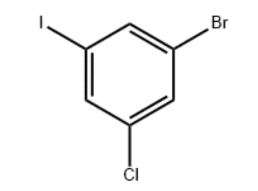
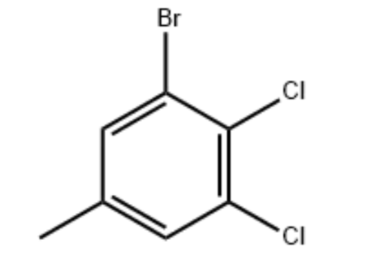
UIVChem has a wide range of photoresist materials, you are welcome to choose from our website. Besides, we also have new OLED intermediate materials for sale, including 1-Bromo-3-chloro-5-iodobenzene_CAS:13101-40-1, 3-Bromo-4,5-dichlorotoluene_CAS:960305-14-0, welcome your inquiry, we will bring you high quality service to bring you satisfactory cooperation.